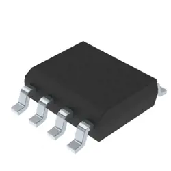

Изображения являются только для ссылки
NCP3063BDR2G
IC REG BUCK BST ADJ 1.5A 8SOIC
- Производитель
- Мфр. Часть #NCP3063BDR2G
- Пакет SOIC-8
- Лист данных
- В наличии7465
100% оригинальный & Новые
24 часа готовы к отправке
Гарантия 365 дней
RFQ и Получить больше скидок
Спецификации
| Package | Tape & Reel (TR),Cut Tape (CT),Bulk |
| ProductStatus | Active |
| Function | Step-Up, Step-Down |
| OutputConfiguration | Positive or Negative |
| Topology | Buck, Boost |
| OutputType | Adjustable |
| NumberofOutputs | 1 |
| Voltage-Input(Min) | 3V |
| Voltage-Input(Max) | 40V |
| Voltage-Output(Min/Fixed) | 1.25V |
| Voltage-Output(Max) | 40V (Switch) |
| Current-Output | 1.5A (Switch) |
| Frequency-Switching | 150kHz |
| SynchronousRectifier | No |
| OperatingTemperature | -40°C ~ 125°C (TJ) |
| MountingType | Surface Mount |
| Package/Case | 8-SOIC (0.154, 3.90mm Width) |
Обзор
Description
Key features include a wide input voltage range, typically from 3 V to 40 V, and the ability to deliver a wide range of output voltages based on the external components used in the circuit. The NCP3063BDR2G is designed with an internal 1.5 A peak current switch, facilitating efficient power conversion while minimizing the number of external components.
The regulator provides built-in protection features such as current limiting and thermal shutdown to enhance reliability and prevent damage under fault conditions. It comes in a compact SOIC-8 package, making it suitable for space-constrained applications in consumer electronics, automotive systems, and industrial equipment. Its adaptability and robust design make it an excellent choice for various power management tasks.
Features
1. Wide Input Voltage Range: It supports a broad input range, typically from 3V to 40V, making it suitable for various applications.
2. Switching Frequency: The device operates at a fixed switching frequency, usually around 150 kHz, ensuring efficient energy conversion.
3. Output Voltage Adjustment: It provides adjustable output voltage through external resistors, offering flexibility in different circuit designs.
4. High Efficiency: The NCP3063BDR2G is designed to deliver high power efficiency, often exceeding 80%, minimizing energy loss.
5. Current Limiting: It features built-in current limiting to protect against overloads and ensures safe operation.
6. Thermal Shutdown: The device includes thermal shutdown protection to prevent damage from overheating.
7. Multiple Configurations: It can be configured for buck, boost, inverting, and flyback topologies, providing versatility for various power supply designs.
8. Package Type: Available in a compact SOIC-8 package, facilitating easy integration on PCBs.
These features make the NCP3063BDR2G suitable for automotive, industrial, and consumer electronics applications requiring reliable and efficient power conversion.
Package
Pinout
1. Pin 1 (IN): Input voltage pin where the unregulated voltage is applied.
2. Pin 2 (SW): Switch collector pin, which connects to the external inductor and diode.
3. Pin 3 (GND): Ground pin, serving as the circuit ground.
4. Pin 4 (Feedback): Receives the feedback voltage from the output through a resistor divider to regulate the output voltage.
5. Pin 5 (ON/OFF): Shutdown pin to enable or disable the device.
6. Pin 6 (Timing Capacitor): Connects to an external capacitor that sets the oscillator frequency.
7. Pin 7 (Current Sense): Connects to a resistor for current limiting and current sense feedback.
8. Pin 8 (VCC): This pin is typically connected internally and not used externally.
These pins serve the purpose of allowing the NCP3063BDR2G to perform its function as a versatile and efficient switching regulator.
Manufacturer
Application
Equivalent
Доставка
Методы доставки Мы
предлагать глобальные услуги доставки через DHL, FedEx, TNT, UPS или любой другой экспедитор по вашему выбору.
Ссылка на плату за доставку (DHL/FedEx):
DHL компанией: Стоимость доставки варьируется от 25 до 45 долларов США (0,5 кг), при этом предполагаемое время доставки составляет 2-5 рабочих дней.
компании FedEx: Стоимость доставки варьируется от 25 до 40 долларов США (0,5 кг), при этом предполагаемое время доставки составляет 3-7 рабочих дней.
УПС: Стоимость доставки варьируется от 25 до 45 долларов США (0,5 кг), при этом предполагаемое время доставки составляет 3-7 рабочих дней.
ТНТ: Стоимость доставки варьируется от 25 до 65 долларов США (0,5 кг), при этом предполагаемое время доставки составляет 3-7 рабочих дней.
ЭМС: Стоимость доставки варьируется от $30-$50 (0,5 кг), с предполагаемым сроком доставки 7-15 рабочих дней.
Зарегистрированная воздушная почта: Стоимость доставки составляет 2-4 доллара США (0,1 кг), при этом предполагаемое время доставки составляет 5-20 рабочих дней.
Платежи
Payment Methods
Срок оплаты 100% предоплаченный.
В настоящее время мы принимаем только следующие способы оплаты:
1. PayPal
2. Кредитная/ дебетовая карта
3. Перевод банковских средств
Похожие
-
![MX25L3233FZBI-08Q]() MX25L3233FZBI-08Q
MX25L3233FZBI-08Q
Macronix
-
![MX66U1G45GXDI00]() MX66U1G45GXDI00
MX66U1G45GXDI00
Macronix
-
![MX25V4035FZUI]() MX25V4035FZUI
MX25V4035FZUI
Macronix
-
![MX30LF2G28AD-TI]() MX30LF2G28AD-TI
MX30LF2G28AD-TI
Macronix
-
![MX25V1635FM2I]() MX25V1635FM2I
MX25V1635FM2I
Macronix
-
![MX25L12833FM2I-10G]() MX25L12833FM2I-10..
MX25L12833FM2I-10..
Macronix
-
![MX25L12833FZNI-10G]() MX25L12833FZNI-10..
MX25L12833FZNI-10..
Macronix
-
![MX25L12835FZ2I-10G]() MX25L12835FZ2I-10..
MX25L12835FZ2I-10..
Macronix
-
![MX29F040CQI-70G]() MX29F040CQI-70G
MX29F040CQI-70G
Macronix
-
![MX29F040CTI-70G]() MX29F040CTI-70G
MX29F040CTI-70G
Macronix
-
![MX30LF4G18AC-TI]() MX30LF4G18AC-TI
MX30LF4G18AC-TI
Macronix
-
![MX25U51245GZ4I00]() MX25U51245GZ4I00
MX25U51245GZ4I00
Macronix