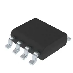

Изображения являются только для ссылки
MAX660ESA+T
IC REG CHARGE PUMP INV 8SOIC
- Производитель
- Мфр. Часть #MAX660ESA+T
- Пакет 8-SOIC
- Лист данных
- В наличии3072
100% оригинальный & Новые
24 часа готовы к отправке
Гарантия 365 дней
RFQ и Получить больше скидок
Спецификации
| Package | Tape & Reel (TR),Cut Tape (CT) |
| ProductStatus | Active |
| Function | Ratiometric |
| OutputConfiguration | Positive or Negative |
| Topology | Charge Pump |
| OutputType | Fixed |
| NumberofOutputs | 1 |
| Voltage-Input(Min) | 1.5V |
| Voltage-Input(Max) | 5.5V |
| Voltage-Output(Min/Fixed) | -Vin, 2Vin |
| Current-Output | 100mA |
| Frequency-Switching | 10kHz, 80kHz |
| SynchronousRectifier | No |
| OperatingTemperature | -40°C ~ 85°C (TA) |
| MountingType | Surface Mount |
| Package/Case | 8-SOIC (0.154, 3.90mm Width) |
Обзор
Description
Key features of the MAX660ESA+T include low quiescent current, high efficiency, and minimal external components. It typically requires only two external capacitors to operate, which simplifies the design and reduces the overall cost of the system. The IC delivers up to 100mA of output current, making it ideal for powering low-current devices.
The MAX660ESA+T comes in an 8-pin SOIC package, ensuring easy integration into various circuit boards. Its versatility and reliability make it suitable for applications like powering operational amplifiers, analog sensors, and microcontrollers. Additionally, built-in features such as thermal shutdown and short-circuit protection enhance its robustness in various operating conditions.
Features
1. Voltage Conversion: Capable of both voltage inversion and doubling, making it versatile for various applications.
2. Input Voltage Range: Operates within a 1.5V to 5.5V input voltage range, suitable for use with standard battery voltages.
3. Efficiency: Offers high power efficiency due to low quiescent current and reduced power dissipation.
4. Output Resistance: Features low output resistance, enhancing its ability to deliver more current to the load.
5. Oscillator Frequency: Operates with a fixed frequency oscillator, simplifying design considerations and reducing output noise.
6. Compact Package: Available in an 8-pin SOIC package, supporting compact design requirements.
7. Shutdown Mode: Includes a shutdown feature to minimize power consumption when the device is not in use.
8. Temperature Range: Operates over a wide temperature range, making it suitable for various environmental conditions.
These features make the MAX660ESA+T suitable for battery-powered devices, LCD bias supplies, and other applications requiring efficient voltage conversion.
Package
Pinout
1. Pin 1 (BOOST): Used to improve the efficiency of the charge pump by connecting a capacitor, boosting the switching frequency.
2. Pin 2 (CAP+): Positive terminal of the flying capacitor used in the charge pump operation.
3. Pin 3 (GND): Ground connection.
4. Pin 4 (CAP-): Negative terminal of the flying capacitor.
5. Pin 5 (OUT): Output voltage, which is the inverted or doubled voltage, depending on the configuration.
6. Pin 6 (LV): Logic-level input that selects between doubling or inverting modes.
7. Pin 7 (IN): Input voltage pin.
8. Pin 8 (OSC): Used to connect a capacitor for setting the oscillator frequency or connecting to an external clock.
This configuration allows the MAX660ESA+T to be used in applications requiring voltage inversion or doubling with a simple external component setup.
Manufacturer
Application
Equivalent
Доставка
Методы доставки Мы
предлагать глобальные услуги доставки через DHL, FedEx, TNT, UPS или любой другой экспедитор по вашему выбору.
Ссылка на плату за доставку (DHL/FedEx):
DHL компанией: Стоимость доставки варьируется от 25 до 45 долларов США (0,5 кг), при этом предполагаемое время доставки составляет 2-5 рабочих дней.
компании FedEx: Стоимость доставки варьируется от 25 до 40 долларов США (0,5 кг), при этом предполагаемое время доставки составляет 3-7 рабочих дней.
УПС: Стоимость доставки варьируется от 25 до 45 долларов США (0,5 кг), при этом предполагаемое время доставки составляет 3-7 рабочих дней.
ТНТ: Стоимость доставки варьируется от 25 до 65 долларов США (0,5 кг), при этом предполагаемое время доставки составляет 3-7 рабочих дней.
ЭМС: Стоимость доставки варьируется от $30-$50 (0,5 кг), с предполагаемым сроком доставки 7-15 рабочих дней.
Зарегистрированная воздушная почта: Стоимость доставки составляет 2-4 доллара США (0,1 кг), при этом предполагаемое время доставки составляет 5-20 рабочих дней.
Платежи
Payment Methods
Срок оплаты 100% предоплаченный.
В настоящее время мы принимаем только следующие способы оплаты:
1. PayPal
2. Кредитная/ дебетовая карта
3. Перевод банковских средств
Похожие
-
![MX25L3233FZBI-08Q]() MX25L3233FZBI-08Q
MX25L3233FZBI-08Q
Macronix
-
![MX25V1635FZNQ03]() MX25V1635FZNQ03
MX25V1635FZNQ03
Macronix
-
![MX25V4035FZUI]() MX25V4035FZUI
MX25V4035FZUI
Macronix
-
![MX25L25673GMI-08G]() MX25L25673GMI-08G
MX25L25673GMI-08G
Macronix
-
![MX25L25673GMI-10G]() MX25L25673GMI-10G
MX25L25673GMI-10G
Macronix
-
![MX29GL512FHXFI-11G]() MX29GL512FHXFI-11..
MX29GL512FHXFI-11..
Macronix
-
![MX25L2006EM1I-12G]() MX25L2006EM1I-12G
MX25L2006EM1I-12G
Macronix
-
![MX25V1635FM2I]() MX25V1635FM2I
MX25V1635FM2I
Macronix
-
![MX25L12833FZ2I-10G]() MX25L12833FZ2I-10..
MX25L12833FZ2I-10..
Macronix
-
![MX29LV160DTTI-70G]() MX29LV160DTTI-70G
MX29LV160DTTI-70G
Macronix
-
![MX29F800CBTI-70G]() MX29F800CBTI-70G
MX29F800CBTI-70G
Macronix
-
![MX29LV640ETTI-70G]() MX29LV640ETTI-70G
MX29LV640ETTI-70G
Macronix