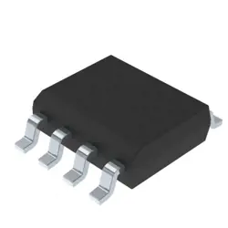
Изображения являются только для ссылки
IPB100N10S3-05
MOSFETs N-Ch 100V 100A D2PAK-2 OptiMOS-T
- Производитель
- Мфр. Часть #IPB100N10S3-05
- Пакет
- Лист данных IPB100N10S3-05 DataSheet
- В наличии3631
100% оригинальный & Новые
24 часа готовы к отправке
Гарантия 365 дней
RFQ и Получить больше скидок
Спецификации
| Packaging | MouseReel |
| Standard Pack Qty | 1000 |
Обзор
Description
The device has a high continuous drain current rating, allowing it to handle significant power loads, making it ideal for use in DC-DC converters, motor drivers, and power switching applications. Its fast switching speed contributes to reduced switching losses, which is critical in high-frequency applications.
The IPB100N10S3-05 is packaged in a TO-220 format, facilitating effective heat dissipation and easy mounting in electronic circuits. Overall, this MOSFET is valued for its reliability and performance in demanding environments, making it a popular choice among engineers for various power electronic designs.
Features
1. Voltage Rating: It has a maximum drain-source voltage (V_DS) of 100V, making it suitable for high-voltage applications.
2. Current Rating: The device can handle a continuous drain current (I_D) of up to 100A, allowing it to efficiently drive heavy loads.
3. Low R_DS(on): With a low on-resistance (R_DS(on)) of approximately 10 mΩ at V_GS of 10V, it ensures minimal power loss during operation.
4. Fast Switching Speed: The MOSFET supports fast switching capabilities, making it ideal for applications requiring high efficiency and speed.
5. Thermal Performance: It has a robust thermal performance, allowing for effective heat dissipation.
6. Package Type: Available in a TO-220 package, facilitating easy mounting and heat management.
These features make the IPB100N10S3-05 suitable for applications in power supplies, motor drives, and DC-DC converters.
Package
Pinout
1. Gate (G): This pin is used to control the MOSFET. A voltage applied to this pin determines whether the device is on or off.
2. Drain (D): This pin is connected to the load. Current flows from the drain to the source when the MOSFET is activated.
3. Source (S): This pin is connected to ground or the lower voltage level of the circuit. It serves as the return path for the current flowing through the MOSFET.
This device is designed for high-efficiency applications, featuring low on-resistance and fast switching capabilities.
Manufacturer
Application
Equivalent
Доставка
Методы доставки Мы
предлагать глобальные услуги доставки через DHL, FedEx, TNT, UPS или любой другой экспедитор по вашему выбору.
Ссылка на плату за доставку (DHL/FedEx):
DHL компанией: Стоимость доставки варьируется от 25 до 45 долларов США (0,5 кг), при этом предполагаемое время доставки составляет 2-5 рабочих дней.
компании FedEx: Стоимость доставки варьируется от 25 до 40 долларов США (0,5 кг), при этом предполагаемое время доставки составляет 3-7 рабочих дней.
УПС: Стоимость доставки варьируется от 25 до 45 долларов США (0,5 кг), при этом предполагаемое время доставки составляет 3-7 рабочих дней.
ТНТ: Стоимость доставки варьируется от 25 до 65 долларов США (0,5 кг), при этом предполагаемое время доставки составляет 3-7 рабочих дней.
ЭМС: Стоимость доставки варьируется от $30-$50 (0,5 кг), с предполагаемым сроком доставки 7-15 рабочих дней.
Зарегистрированная воздушная почта: Стоимость доставки составляет 2-4 доллара США (0,1 кг), при этом предполагаемое время доставки составляет 5-20 рабочих дней.
Платежи
Payment Methods
Срок оплаты 100% предоплаченный.
В настоящее время мы принимаем только следующие способы оплаты:
1. PayPal
2. Кредитная/ дебетовая карта
3. Перевод банковских средств
Похожие
-
![MX25R8035FM1IL0]() MX25R8035FM1IL0
Macronix
-
![MX25L3233FM1I-08Q]() MX25L3233FM1I-08Q
Macronix
-
![MX25V1635FZNQ03]() MX25V1635FZNQ03
Macronix
-
![MX25V4035FZUI]() MX25V4035FZUI
Macronix
-
![MX25V2033FM1I]() MX25V2033FM1I
Macronix
-
![MX25V16066M2I02]() MX25V16066M2I02
Macronix
-
![MX25L25673GMI-10G]() MX25L25673GMI-10G
Macronix
-
![MX29GL512FHXFI-11G]() MX29GL512FHXFI-11..
Macronix
-
![MX25U51279GXDR00]() MX25U51279GXDR00
Macronix
-
![MX25U25643GZNI00]() MX25U25643GZNI00
Macronix
-
![MX25R1635FZUIH0]() MX25R1635FZUIH0
Macronix
-
![MX25V1635FM2I]() MX25V1635FM2I
Macronix