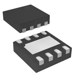
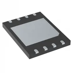
Изображения являются только для ссылки
BL24C02F-PARC
- Производитель
- Мфр. Часть #BL24C02F-PARC
- Пакет
- Лист данных BL24C02F-PARC DataSheet
- В наличии25457
100% оригинальный & Новые
24 часа готовы к отправке
Гарантия 365 дней
RFQ и Получить больше скидок
Спецификации
| Manufacturer | BL(Shanghai Belling) |
| Package | SOP-8 |
Обзор
Description
Key features include a wide operating voltage range, low power consumption, and fast access times. The device supports multiple addressing modes and has built-in write protection, enhancing data integrity during operation. Its compact package size and reliability make it ideal for embedded systems where space and power efficiency are critical.
Overall, the BL24C02F-PARC provides a versatile solution for applications needing compact and efficient non-volatile memory storage.
Features
1. Interface: Supports I²C protocol for easy integration and communication with microcontrollers.
2. Operating Voltage: Typically operates in a voltage range of 1.8V to 5.5V, making it suitable for low-power applications.
3. Memory Organization: Configured as 256 bytes with 8-bit word size, allowing for efficient data handling.
4. Write Endurance: Offers up to 1 million write cycles per memory cell, ensuring durability for frequent data updates.
5. Data Retention: Guarantees data retention of up to 100 years under proper conditions, ensuring long-term reliability.
6. Package Type: Available in various package options, including SOP and DFN, facilitating easy integration into different designs.
7. Self-Timed Write Cycle: Features a self-timed write cycle, simplifying the control logic for write operations.
These features make the BL24C02F-PARC ideal for applications in consumer electronics, automotive systems, and industrial automation where reliable data storage is essential.
Package
Pinout
The pin functions are as follows:
1. VCC: Power supply voltage.
2. GND: Ground reference.
3. SDA: Serial data line for data communication.
4. SCL: Serial clock line for timing of data transmission.
5. WP: Write protect pin, which prevents writing to the memory when high.
6. A0: Address input pin for chip selection (used in multiple device configurations).
7. A1: Secondary address input for additional device selection.
8. NC: No connection (not used).
This device operates using the I²C interface for communication, allowing easy integration into various electronic applications.
Manufacturer
Application
Equivalent
Доставка
Методы доставки Мы
предлагать глобальные услуги доставки через DHL, FedEx, TNT, UPS или любой другой экспедитор по вашему выбору.
Ссылка на плату за доставку (DHL/FedEx):
DHL компанией: Стоимость доставки варьируется от 25 до 45 долларов США (0,5 кг), при этом предполагаемое время доставки составляет 2-5 рабочих дней.
компании FedEx: Стоимость доставки варьируется от 25 до 40 долларов США (0,5 кг), при этом предполагаемое время доставки составляет 3-7 рабочих дней.
УПС: Стоимость доставки варьируется от 25 до 45 долларов США (0,5 кг), при этом предполагаемое время доставки составляет 3-7 рабочих дней.
ТНТ: Стоимость доставки варьируется от 25 до 65 долларов США (0,5 кг), при этом предполагаемое время доставки составляет 3-7 рабочих дней.
ЭМС: Стоимость доставки варьируется от $30-$50 (0,5 кг), с предполагаемым сроком доставки 7-15 рабочих дней.
Зарегистрированная воздушная почта: Стоимость доставки составляет 2-4 доллара США (0,1 кг), при этом предполагаемое время доставки составляет 5-20 рабочих дней.
Платежи
Payment Methods
Срок оплаты 100% предоплаченный.
В настоящее время мы принимаем только следующие способы оплаты:
1. PayPal
2. Кредитная/ дебетовая карта
3. Перевод банковских средств
Похожие
-
![MX25R8035FM1IL0]() MX25R8035FM1IL0
Macronix
-
![MX25V1635FZNI]() MX25V1635FZNI
Macronix
-
![MX29F400CBTI-70G]() MX29F400CBTI-70G
Macronix
-
![MX66U1G45GXDI00]() MX66U1G45GXDI00
Macronix
-
![MX25V4035FZUI]() MX25V4035FZUI
Macronix
-
![MX25V2033FM1I]() MX25V2033FM1I
Macronix
-
![MX25V16066M1I02]() MX25V16066M1I02
Macronix
-
![MX25R3235FZNIL0]() MX25R3235FZNIL0
Macronix
-
![MX25L25673GMI-08G]() MX25L25673GMI-08G
Macronix
-
![MX25L2006EM1I-12G]() MX25L2006EM1I-12G
Macronix
-
![MX25U3232FZBI02]() MX25U3232FZBI02
Macronix
-
![MX25L12835FZ2I-10G]() MX25L12835FZ2I-10..
Macronix