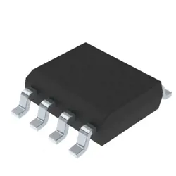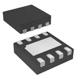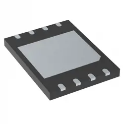

Изображения являются только для ссылки
ADCMP361YRJZ
ADI Dual Comparator & Reference
- Производитель
- Мфр. Часть #ADCMP361YRJZ
- Пакет
- Лист данных
- В наличии21406
100% оригинальный & Новые
24 часа готовы к отправке
Гарантия 365 дней
RFQ и Получить больше скидок
Спецификации
| Packaging | Reel |
| Standard Pack Qty | 3000 |
Обзор
Description
This comparator includes an open-collector output, allowing it to interface easily with other digital devices and logic levels. It also has a high common-mode input voltage range, making it versatile for various circuit designs. The device operates over a wide temperature range, ensuring reliability in diverse environmental conditions.
The ADCMP361YRJZ is commonly used in telecommunications, automotive, instrumentation, and consumer electronics. Its compact package and efficient design make it ideal for space-constrained applications. Overall, it provides a reliable solution for high-speed signal comparison tasks.
Features
1. Single-Supply Operation: It operates from a single supply voltage, typically ranging from 2.0V to 5.5V, enhancing design flexibility.
2. High Speed: Offers a propagation delay of around 4 ns, making it suitable for high-frequency applications.
3. Low Power Consumption: It consumes only 1.5 mA, allowing for energy-efficient designs.
4. TTL/CMOS Compatible Outputs: The output can directly drive TTL or CMOS logic, simplifying integration into digital systems.
5. Wide Input Common Mode Range: Supports a common mode range that extends from ground to V+ - 1.5V, accommodating various signal levels.
6. Hysteresis: Features built-in hysteresis to improve noise immunity and prevent oscillations.
7. Applications: Ideal for applications such as zero-crossing detectors, signal conditioning, and high-speed data communications.
Overall, the ADCMP361YRJZ is designed for precision and speed in a compact package.
Package
Pinout
1. VDD (Pin 1): Power supply input.
2. GND (Pin 2): Ground reference.
3. Inverting Input (V-) (Pin 3): Negative input for comparison.
4. Non-Inverting Input (V+) (Pin 4): Positive input for comparison.
5. Output (OUT) (Pin 5): Output signal indicating the comparison result.
6. NC (Pin 6): No Connect - not used.
7. VREF (Pin 7): Reference voltage input.
8. Compensation Pin (C) (Pin 8): For internal compensation to stabilize performance.
This device is suitable for applications requiring high-speed response and low power consumption.
Manufacturer
Application
Equivalent
Доставка
Методы доставки Мы
предлагать глобальные услуги доставки через DHL, FedEx, TNT, UPS или любой другой экспедитор по вашему выбору.
Ссылка на плату за доставку (DHL/FedEx):
DHL компанией: Стоимость доставки варьируется от 25 до 45 долларов США (0,5 кг), при этом предполагаемое время доставки составляет 2-5 рабочих дней.
компании FedEx: Стоимость доставки варьируется от 25 до 40 долларов США (0,5 кг), при этом предполагаемое время доставки составляет 3-7 рабочих дней.
УПС: Стоимость доставки варьируется от 25 до 45 долларов США (0,5 кг), при этом предполагаемое время доставки составляет 3-7 рабочих дней.
ТНТ: Стоимость доставки варьируется от 25 до 65 долларов США (0,5 кг), при этом предполагаемое время доставки составляет 3-7 рабочих дней.
ЭМС: Стоимость доставки варьируется от $30-$50 (0,5 кг), с предполагаемым сроком доставки 7-15 рабочих дней.
Зарегистрированная воздушная почта: Стоимость доставки составляет 2-4 доллара США (0,1 кг), при этом предполагаемое время доставки составляет 5-20 рабочих дней.
Платежи
Payment Methods
Срок оплаты 100% предоплаченный.
В настоящее время мы принимаем только следующие способы оплаты:
1. PayPal
2. Кредитная/ дебетовая карта
3. Перевод банковских средств
Похожие
-
![MX25R8035FM1IL0]() MX25R8035FM1IL0
MX25R8035FM1IL0
Macronix
-
![MX25V1635FZNQ03]() MX25V1635FZNQ03
MX25V1635FZNQ03
Macronix
-
![MX29F400CBTI-70G]() MX29F400CBTI-70G
MX29F400CBTI-70G
Macronix
-
![MX25V2033FM1I]() MX25V2033FM1I
MX25V2033FM1I
Macronix
-
![MX25V16066M1I02]() MX25V16066M1I02
MX25V16066M1I02
Macronix
-
![MX29GL512FHXFI-11G]() MX29GL512FHXFI-11..
MX29GL512FHXFI-11..
Macronix
-
![MX25U51279GXDR00]() MX25U51279GXDR00
MX25U51279GXDR00
Macronix
-
![MX25L2006EM1I-12G]() MX25L2006EM1I-12G
MX25L2006EM1I-12G
Macronix
-
![MX25V1635FM2I]() MX25V1635FM2I
MX25V1635FM2I
Macronix
-
![MX25U3232FZBI02]() MX25U3232FZBI02
MX25U3232FZBI02
Macronix
-
![MX25L12833FM2I-10G]() MX25L12833FM2I-10..
MX25L12833FM2I-10..
Macronix
-
![MX25L12833FZ2I-10G]() MX25L12833FZ2I-10..
MX25L12833FZ2I-10..
Macronix