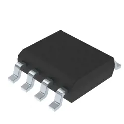

Изображения являются только для ссылки
74LVC2G17GW
Buffers & Line Drivers
- Производитель
- Мфр. Часть #74LVC2G17GW
- Пакет
- Лист данных
- В наличии5131
100% оригинальный & Новые
24 часа готовы к отправке
Гарантия 365 дней
RFQ и Получить больше скидок
Спецификации
Обзор
Description
Key features include a supply voltage range of 1.65V to 5.5V, low power consumption, and high noise immunity. The 74LVC2G17GW is implemented in a small form factor, typically available in a SOT-23 package, making it suitable for space-constrained applications. With its CMOS technology, it supports fast switching times and low propagation delay, making it ideal for use in portable devices, communication systems, and other digital applications that require efficient signal management. The device is also compatible with various logic levels, ensuring versatility in integration with other components.
Features
- Voltage Range: Operates with a supply voltage of 1.65V to 5.5V, making it suitable for both 3.3V and 5V systems.
- Low Power Consumption: The device has a low static and dynamic power consumption, enhancing energy efficiency.
- High-Speed Performance: Offers fast propagation delays, typically around 4.5 ns at 3.3V and a load of 50 pF.
- Input Compatibility: Accepts TTL input levels, ensuring compatibility with various logic families.
- Output Characteristics: Features fully-static outputs that can drive up to 32 mA at VCC = 3.3V.
- Compact Package: Available in a small form factor SOT-23 package, ideal for space-constrained applications.
- ESD Protection: Built-in ESD protection enhances reliability in sensitive environments.
This makes the 74LVC2G17GW suitable for a wide range of digital circuit applications, including portable devices and battery-operated systems.
Package
Pinout
Pin Functions:
1. 1A (Input for Buffer 1) - Input for the first buffer.
2. 1Y (Output for Buffer 1) - Output for the first buffer.
3. 2A (Input for Buffer 2) - Input for the second buffer.
4. 2Y (Output for Buffer 2) - Output for the second buffer.
5. GND (Ground) - Connects to the ground.
6. VCC (Power Supply) - Connects to the positive voltage supply.
The device is designed for low-voltage operation (1.65V to 5.5V) and is suitable for use in various digital circuits requiring signal buffering with a Schmitt-trigger feature.
Manufacturer
Application
Equivalent
1. 74LVC2G02 (dual 2-input NOR gate)
2. 74HC02 (dual 2-input NOR gate, high-speed CMOS)
3. 74HCT02 (dual 2-input NOR gate, TTL-compatible)
For direct equivalence in functionality, look for other dual 2-input NAND gates from LVC, HC, or HCT families, like 74HC20 or 74HCT20, depending on voltage and speed requirements. Always verify the specific pin configurations and voltage levels.
Доставка
Методы доставки Мы
предлагать глобальные услуги доставки через DHL, FedEx, TNT, UPS или любой другой экспедитор по вашему выбору.
Ссылка на плату за доставку (DHL/FedEx):
DHL компанией: Стоимость доставки варьируется от 25 до 45 долларов США (0,5 кг), при этом предполагаемое время доставки составляет 2-5 рабочих дней.
компании FedEx: Стоимость доставки варьируется от 25 до 40 долларов США (0,5 кг), при этом предполагаемое время доставки составляет 3-7 рабочих дней.
УПС: Стоимость доставки варьируется от 25 до 45 долларов США (0,5 кг), при этом предполагаемое время доставки составляет 3-7 рабочих дней.
ТНТ: Стоимость доставки варьируется от 25 до 65 долларов США (0,5 кг), при этом предполагаемое время доставки составляет 3-7 рабочих дней.
ЭМС: Стоимость доставки варьируется от $30-$50 (0,5 кг), с предполагаемым сроком доставки 7-15 рабочих дней.
Зарегистрированная воздушная почта: Стоимость доставки составляет 2-4 доллара США (0,1 кг), при этом предполагаемое время доставки составляет 5-20 рабочих дней.
Платежи
Payment Methods
Срок оплаты 100% предоплаченный.
В настоящее время мы принимаем только следующие способы оплаты:
1. PayPal
2. Кредитная/ дебетовая карта
3. Перевод банковских средств
Похожие
-
![MX25V5126FM1I]() MX25V5126FM1I
MX25V5126FM1I
Macronix
-
![MX25V4035FZUI]() MX25V4035FZUI
MX25V4035FZUI
Macronix
-
![MX25R3235FZNIL0]() MX25R3235FZNIL0
MX25R3235FZNIL0
Macronix
-
![MX25V16066M2I02]() MX25V16066M2I02
MX25V16066M2I02
Macronix
-
![MX25R1635FZUIH0]() MX25R1635FZUIH0
MX25R1635FZUIH0
Macronix
-
![MX25V1635FM2I]() MX25V1635FM2I
MX25V1635FM2I
Macronix
-
![MX25L6433FM2I-08G]() MX25L6433FM2I-08G
MX25L6433FM2I-08G
Macronix
-
![MX25U6435FM2I-10G]() MX25U6435FM2I-10G
MX25U6435FM2I-10G
Macronix
-
![MX25L12833FZ2I-10G]() MX25L12833FZ2I-10..
MX25L12833FZ2I-10..
Macronix
-
![MX25L12833FZNI-10G]() MX25L12833FZNI-10..
MX25L12833FZNI-10..
Macronix
-
![MX29F040CQI-70G]() MX29F040CQI-70G
MX29F040CQI-70G
Macronix
-
![MX25L25645GXDI-08G]() MX25L25645GXDI-08..
MX25L25645GXDI-08..
Macronix