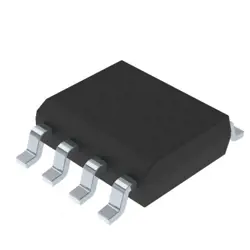

Изображения являются только для ссылки
74LVC1G79GW-Q100H
IC FF D-TYPE SNGL 1BIT 5TSSOP
- Производитель
- Мфр. Часть #74LVC1G79GW-Q100H
- Пакет
- Лист данных 74LVC1G79GW-Q100H DataSheet
- В наличии2937
100% оригинальный & Новые
24 часа готовы к отправке
Гарантия 365 дней
RFQ и Получить больше скидок
Спецификации
| Package | Tape & Reel (TR) |
| Series | Automotive, AEC-Q100, 74LVC |
| ProductStatus | Active |
| Function | Standard |
| Type | D-Type |
| OutputType | Non-Inverted |
| NumberofElements | 1 |
| NumberofBitsperElement | 1 |
| ClockFrequency | 500 MHz |
| MaxPropagationDelay@VMaxCL | 3.8ns @ 5V, 50pF |
| TriggerType | Positive Edge |
| Current-OutputHighLow | 32mA, 32mA |
| Voltage-Supply | 1.65V ~ 5.5V |
| Current-Quiescent(Iq) | 4 µA |
| InputCapacitance | 5 pF |
| OperatingTemperature | -40°C ~ 125°C (TA) |
| MountingType | Surface Mount |
| SupplierDevicePackage | 5-TSSOP |
Обзор
Description
The tri-state output can be in one of three states: high, low, or high-impedance, allowing multiple outputs to connect to a common bus without interference. Its compact package (typically a SOT23-5) makes it ideal for space-constrained designs, such as in portable electronics. The 74LVC1G79GW-Q100H also features low static and dynamic power consumption, making it efficient for battery-operated devices.
Overall, the 74LVC1G79GW-Q100H is a versatile component widely used in various applications, including data communication, signal processing, and control systems.
Features
1. Voltage Range: Operates from 1.65V to 5.5V, making it suitable for various logic levels.
2. High Speed: Offers fast switching times (typically under 5 ns at 3.3V).
3. Low Power Consumption: Consumes minimal power, making it ideal for battery-operated devices.
4. Low Input/Output Capacitance: Ensures efficient signal transmission.
5. TTL Compatible: Compatible with TTL levels, enhancing integration into existing designs.
6. Power-down Mode: Features a power-down mode for reduced power consumption.
7. ESD Protection: Robust against electrostatic discharge, improving reliability.
8. Small Package: Available in a compact SOT-23-5 package, saving board space.
The 74LVC1G79GW-Q100H is ideal for applications requiring reliable logic functions with stringent power and speed requirements.
Package
Pinout
Pin Functions:
1. Pin 1 (A): Input A
2. Pin 2 (B): Input B
3. Pin 3 (S): Select input
4. Pin 4 (Y): Output
5. Pin 5 (GND): Ground
The device allows selection between two input signals (A and B) based on the state of the select input (S). If S is low, the output Y reflects the value of input A; if S is high, Y reflects input B. This multiplexer operates with supply voltages in the range of 1.65V to 5.5V, making it suitable for various low-voltage applications.
Manufacturer
Application
Equivalent
1. 74LVC1G79 (without specific temperature grade or packaging)
2. 74HC1G79 (higher supply voltage range, not Schmitt-trigger)
3. 74HCT1G79 (TTL-compatible input levels)
Always verify specifications for exact compatibility.
Доставка
Методы доставки Мы
предлагать глобальные услуги доставки через DHL, FedEx, TNT, UPS или любой другой экспедитор по вашему выбору.
Ссылка на плату за доставку (DHL/FedEx):
DHL компанией: Стоимость доставки варьируется от 25 до 45 долларов США (0,5 кг), при этом предполагаемое время доставки составляет 2-5 рабочих дней.
компании FedEx: Стоимость доставки варьируется от 25 до 40 долларов США (0,5 кг), при этом предполагаемое время доставки составляет 3-7 рабочих дней.
УПС: Стоимость доставки варьируется от 25 до 45 долларов США (0,5 кг), при этом предполагаемое время доставки составляет 3-7 рабочих дней.
ТНТ: Стоимость доставки варьируется от 25 до 65 долларов США (0,5 кг), при этом предполагаемое время доставки составляет 3-7 рабочих дней.
ЭМС: Стоимость доставки варьируется от $30-$50 (0,5 кг), с предполагаемым сроком доставки 7-15 рабочих дней.
Зарегистрированная воздушная почта: Стоимость доставки составляет 2-4 доллара США (0,1 кг), при этом предполагаемое время доставки составляет 5-20 рабочих дней.
Платежи
Payment Methods
Срок оплаты 100% предоплаченный.
В настоящее время мы принимаем только следующие способы оплаты:
1. PayPal
2. Кредитная/ дебетовая карта
3. Перевод банковских средств
Похожие
-
![MX25L3233FZBI-08Q]() MX25L3233FZBI-08Q
MX25L3233FZBI-08Q
Macronix
-
![MX25V1635FZNI]() MX25V1635FZNI
MX25V1635FZNI
Macronix
-
![MX25V16066M1I02]() MX25V16066M1I02
MX25V16066M1I02
Macronix
-
![MX25V16066M2I02]() MX25V16066M2I02
MX25V16066M2I02
Macronix
-
![MX25L25673GMI-08G]() MX25L25673GMI-08G
MX25L25673GMI-08G
Macronix
-
![MX25L25673GMI-10G]() MX25L25673GMI-10G
MX25L25673GMI-10G
Macronix
-
![MX29GL512FHXFI-11G]() MX29GL512FHXFI-11..
MX29GL512FHXFI-11..
Macronix
-
![MX25U51279GXDR00]() MX25U51279GXDR00
MX25U51279GXDR00
Macronix
-
![MX25V1635FM2I]() MX25V1635FM2I
MX25V1635FM2I
Macronix
-
![MX29F040CQI-70G]() MX29F040CQI-70G
MX29F040CQI-70G
Macronix
-
![MX29F040CTI-70G]() MX29F040CTI-70G
MX29F040CTI-70G
Macronix
-
![MX29LV640ETTI-70G]() MX29LV640ETTI-70G
MX29LV640ETTI-70G
Macronix