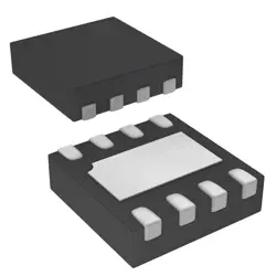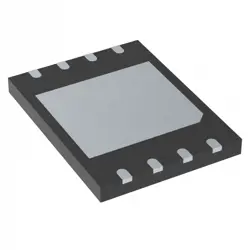

Изображения являются только для ссылки
74LVC1G79GW
D FLIP-FLOP, LVC/LCX/Z SERIES, 1
- Производитель
- Мфр. Часть #74LVC1G79GW
- Пакет
- Лист данных 74LVC1G79GW DataSheet
- В наличии6437
100% оригинальный & Новые
24 часа готовы к отправке
Гарантия 365 дней
RFQ и Получить больше скидок
Спецификации
| Package | Bulk |
| ProductStatus | Active |
Обзор
Description
The 74LVC1G79GW comes in a small, space-efficient package, such as the TSSOP or DFN, making it ideal for compact circuit designs. Its low power consumption and high noise immunity make it suitable for battery-powered and portable applications. Additionally, the device supports partial power-down mode, which allows it to be used in systems where power conservation is critical. Its robustness, versatility, and ease of integration make the 74LVC1G79GW a popular choice for implementing synchronous data storage elements in digital electronics.
Features
It supports a clock input that triggers on the rising edge, and it has Schmitt-trigger action inputs which provides better noise immunity. The flip-flop is capable of high-speed operation, with a typical propagation delay time of around 3.2 ns at 5 V. It comes in a leadless package type, such as TSSOP, making it suitable for compact circuit designs. Additionally, the 74LVC1G79GW provides ESD protection, which enhances its robustness in industrial and consumer applications. Overall, its compact size, wide voltage range, and efficient performance make it suitable for portable and battery-powered devices.
Package
Pinout
The pin functions are as follows:
1. Pin 1 (D): Data input. The data on this pin is transferred to the Q output on the rising edge of the clock signal.
2. Pin 2 (GND): Ground. This is the common ground reference for the device.
3. Pin 3 (CP): Clock input. The flip-flop captures the data from the D input on the rising edge of this clock signal.
4. Pin 4 (Q): Data output. This pin reflects the state of the D input after the clock signal has triggered.
5. Pin 5 (Q̅): Inverted data output. This pin provides the inverse of the data present at the Q output.
6. Pin 6 (VCC): Power supply. This pin is connected to the positive supply voltage.
The 74LVC1G79GW is commonly used in digital circuits for data storage and transfer applications.
Manufacturer
Application
Equivalent
1. SN74LVC1G79 from Texas Instruments
2. NXP's 74LVC1G79GV
3. Microchip's 74LVC1G79
4. ON Semiconductor's NL17SZ74
Ensure to compare datasheets for specific operational characteristics and package types.
Доставка
Методы доставки Мы
предлагать глобальные услуги доставки через DHL, FedEx, TNT, UPS или любой другой экспедитор по вашему выбору.
Ссылка на плату за доставку (DHL/FedEx):
DHL компанией: Стоимость доставки варьируется от 25 до 45 долларов США (0,5 кг), при этом предполагаемое время доставки составляет 2-5 рабочих дней.
компании FedEx: Стоимость доставки варьируется от 25 до 40 долларов США (0,5 кг), при этом предполагаемое время доставки составляет 3-7 рабочих дней.
УПС: Стоимость доставки варьируется от 25 до 45 долларов США (0,5 кг), при этом предполагаемое время доставки составляет 3-7 рабочих дней.
ТНТ: Стоимость доставки варьируется от 25 до 65 долларов США (0,5 кг), при этом предполагаемое время доставки составляет 3-7 рабочих дней.
ЭМС: Стоимость доставки варьируется от $30-$50 (0,5 кг), с предполагаемым сроком доставки 7-15 рабочих дней.
Зарегистрированная воздушная почта: Стоимость доставки составляет 2-4 доллара США (0,1 кг), при этом предполагаемое время доставки составляет 5-20 рабочих дней.
Платежи
Payment Methods
Срок оплаты 100% предоплаченный.
В настоящее время мы принимаем только следующие способы оплаты:
1. PayPal
2. Кредитная/ дебетовая карта
3. Перевод банковских средств
Похожие
-
![MX25L3233FM1I-08Q]() MX25L3233FM1I-08Q
MX25L3233FM1I-08Q
Macronix
-
![MX29F400CBTI-70G]() MX29F400CBTI-70G
MX29F400CBTI-70G
Macronix
-
![MX25V2033FM1I]() MX25V2033FM1I
MX25V2033FM1I
Macronix
-
![MX25V16066M2I02]() MX25V16066M2I02
MX25V16066M2I02
Macronix
-
![MX30LF2G28AD-TI]() MX30LF2G28AD-TI
MX30LF2G28AD-TI
Macronix
-
![MX25L8035EM2I-10G]() MX25L8035EM2I-10G
MX25L8035EM2I-10G
Macronix
-
![MX25U51279GXDR00]() MX25U51279GXDR00
MX25U51279GXDR00
Macronix
-
![MX25U25643GZNI00]() MX25U25643GZNI00
MX25U25643GZNI00
Macronix
-
![MX25U3232FZBI02]() MX25U3232FZBI02
MX25U3232FZBI02
Macronix
-
![MX25L6433FM2I-08G]() MX25L6433FM2I-08G
MX25L6433FM2I-08G
Macronix
-
![MX25L12833FZ2I-10G]() MX25L12833FZ2I-10..
MX25L12833FZ2I-10..
Macronix
-
![MX25L12833FZNI-10G]() MX25L12833FZNI-10..
MX25L12833FZNI-10..
Macronix