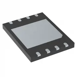
Изображения являются только для ссылки
74LV595PW
- Производитель
- Мфр. Часть #74LV595PW
- Пакет
- Лист данных
- В наличии4320
100% оригинальный & Новые
24 часа готовы к отправке
Гарантия 365 дней
RFQ и Получить больше скидок
Спецификации
| Shipping Restrictions | Mouser does not presently sell this product in your region. |
| Counting Sequence | Serial to Serial/Parallel |
| Number of Circuits | 1 Circuit |
| Number of Bits | 8 bit |
| Package / Case | TSSOP-16 |
| Logic Family | LV |
| Logic Type | CMOS |
| Number of Input Lines | 1 |
| Propagation Delay Time | 100 ns, 34 ns |
| Supply Voltage - Min | 1 V |
| Supply Voltage - Max | 3.6 V |
| Minimum Operating Temperature | - 40 C |
| Maximum Operating Temperature | + 125 C |
| Brand | Nexperia |
| Function | Shift Register |
| Mounting Style | SMD/SMT |
| Number of Output Lines | 9 Line |
| Product Type | Counter Shift Registers |
| Factory Pack Quantity:Factory Pack Quantity | 96 |
| Subcategory | Logic ICs |
| Width | 4.5 mm |
| Part # Aliases | 74LV595PW,112 |
| Unit Weight | 0.006102 oz |
| Operating Supply Voltage | 3.3 V |
| Height | 0.95 mm |
| Length | 5.1 mm |
| Supply Current - Max | 160 uA |
| Output Type | 3-State |
| Features | No Parallel Enable Input |
| Reset Type | Asynchronous |
| Triggering Type | Positive-Edge |
Обзор
Description
The 74LV595PW features an 8-bit shift register and an 8-bit storage register, which are both positive-edge-triggered. Data is shifted on the rising edge of the clock input, and it can be transferred to the output register either serially or in parallel. The outputs can be set to high-impedance, ensuring that multiple devices can share the same data lines.
This IC is often used in LED displays, data acquisition systems, and microcontroller interfacing to expand GPIO pins. It's encapsulated in a TSSOP (Thin Shrink Small Outline Package), which is compact and suitable for space-constrained applications. The device is part of the 74LV series, which is known for its low-voltage, low-power operation, and performance consistency across varying temperature ranges.
Features
1. Low Voltage Operation: Operates at a voltage range of 1.0 V to 5.5 V, making it suitable for a wide variety of low-power applications.
2. High-Speed Operation: The device supports high-speed data transfer, facilitating rapid operation in digital circuits.
3. Serial Input and Parallel Output: Allows data to be input serially and output in parallel, useful for expanding I/O capabilities.
4. 3-State Outputs: The outputs can be set to a high-impedance state, allowing for easy bus interfacing and minimizing power consumption.
5. Latch Functionality: Data can be latched to maintain output even after the input data changes, providing stable performance.
6. Low Power Consumption: The device is designed to consume minimal power, ideal for battery-operated applications.
7. Wide Temperature Range: It operates effectively over a wide temperature range, ensuring reliability in various environments.
These features make the 74LV595PW versatile for use in digital circuits requiring efficient data handling and expansion.
Package
Pinout
Here is a brief overview of its pin functions:
1. Q0-Q7 (Pins 15, 1-7): Parallel output pins.
2. VCC (Pin 16): Supply voltage pin.
3. GND (Pin 8): Ground pin.
4. SER (Pin 14): Serial data input.
5. SRCLK (Pin 11): Shift register clock input, latching data into the shift register on the rising edge.
6. RCLK (Pin 12): Register clock input, transferring data from the shift register to the storage register on the rising edge.
7. /OE (Pin 13): Output enable, active low; controls the output buffers.
8. /SRCLR (Pin 10): Shift register clear, active low; clears the shift register when low.
The 74LV595PW is commonly used for cascading multiple shift registers to increase the number of I/O pins in digital systems.
Manufacturer
Application
Equivalent
1. 74HC595N - NXP
2. SN74HC595 - Texas Instruments
3. MC74HC595ADTR2G - ON Semiconductor
4. CD74HC595M96 - Texas Instruments
5. TC74HC595AP - Toshiba
These components offer similar functionality with variations in electrical characteristics and packaging, so check compatibility with your specific application.
Доставка
Методы доставки Мы
предлагать глобальные услуги доставки через DHL, FedEx, TNT, UPS или любой другой экспедитор по вашему выбору.
Ссылка на плату за доставку (DHL/FedEx):
DHL компанией: Стоимость доставки варьируется от 25 до 45 долларов США (0,5 кг), при этом предполагаемое время доставки составляет 2-5 рабочих дней.
компании FedEx: Стоимость доставки варьируется от 25 до 40 долларов США (0,5 кг), при этом предполагаемое время доставки составляет 3-7 рабочих дней.
УПС: Стоимость доставки варьируется от 25 до 45 долларов США (0,5 кг), при этом предполагаемое время доставки составляет 3-7 рабочих дней.
ТНТ: Стоимость доставки варьируется от 25 до 65 долларов США (0,5 кг), при этом предполагаемое время доставки составляет 3-7 рабочих дней.
ЭМС: Стоимость доставки варьируется от $30-$50 (0,5 кг), с предполагаемым сроком доставки 7-15 рабочих дней.
Зарегистрированная воздушная почта: Стоимость доставки составляет 2-4 доллара США (0,1 кг), при этом предполагаемое время доставки составляет 5-20 рабочих дней.
Платежи
Payment Methods
Срок оплаты 100% предоплаченный.
В настоящее время мы принимаем только следующие способы оплаты:
1. PayPal
2. Кредитная/ дебетовая карта
3. Перевод банковских средств
Похожие
-
![MX25R8035FM1IL0]() MX25R8035FM1IL0
Macronix
-
![MX25L3233FZBI-08Q]() MX25L3233FZBI-08Q
Macronix
-
![MX30LF2G28AD-TI]() MX30LF2G28AD-TI
Macronix
-
![MX25R6435FBDIL0]() MX25R6435FBDIL0
Macronix
-
![MX25L25673GMI-10G]() MX25L25673GMI-10G
Macronix
-
![MX25U25643GZNI00]() MX25U25643GZNI00
Macronix
-
![MX25R1635FZUIH0]() MX25R1635FZUIH0
Macronix
-
![MX25L12833FZ2I-10G]() MX25L12833FZ2I-10..
Macronix
-
![MX29F040CQI-70G]() MX29F040CQI-70G
Macronix
-
![MX25L25645GXDI-08G]() MX25L25645GXDI-08..
Macronix
-
![MX29LV640ETTI-70G]() MX29LV640ETTI-70G
Macronix
-
![MX25L25735FMI-10G]() MX25L25735FMI-10G
Macronix