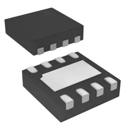

Изображения являются только для ссылки
74AUP1G07GW
Buffers & Line Drivers
- Производитель
- Мфр. Часть #74AUP1G07GW
- Пакет
- Лист данных
- В наличии23657
100% оригинальный & Новые
24 часа готовы к отправке
Гарантия 365 дней
RFQ и Получить больше скидок
Спецификации
Обзор
Description
The buffer/driver is designed to improve signal integrity and drive capability, making it ideal for interfacing different logic levels in systems. It can be used in various applications, including portable electronics, communication devices, and automotive systems. The 74AUP1G07GW comes in a compact SOT-23 package, facilitating easy integration into PCB layouts while minimizing space requirements. Its robustness and versatility make it a popular choice in the realm of digital logic design.
Features
1. Voltage Range: Operates within a supply voltage range of 0.8V to 3.6V, making it suitable for battery-powered devices.
2. Input and Output Compatibility: Compatible with both standard CMOS levels and TTL levels, enhancing versatility in mixed-signal environments.
3. Low Power Consumption: Offers a low static power dissipation, which is essential for energy-efficient designs.
4. High Noise Immunity: The Schmitt-trigger design provides excellent noise immunity and clean signal transitions, reducing susceptibility to spurious signals.
5. Compact Package: Available in a small SOT-23 package, facilitating space-constrained applications.
6. Fast Switching Speed: Ensures quick response times, improving overall circuit performance.
This component is ideal for use in various digital applications like signal conditioning, level shifting, and interfacing in low-power electronic designs.
Package
Pinout
Pin Configuration:
1. A (Input) - This is the data input pin.
2. OE (Output Enable) - This pin controls the output state; when low, the output is enabled, and when high, the output is in a high-impedance state.
3. Y (Output) - This is the buffered output that reflects the input state when the output is enabled.
4. VCC (Power Supply) - The supply voltage pin, typically operates between 0.8V and 3.6V.
5. GND (Ground) - The ground pin.
Functionality:
The device acts as a logic level buffer, allowing for signal amplification and providing output isolation when not enabled. It is suitable for low-voltage applications and is part of the AUP (Advanced Ultra Low Power) logic family, making it energy-efficient.
For further details, refer to the manufacturer's datasheet.
Manufacturer
Application
Equivalent
Доставка
Методы доставки Мы
предлагать глобальные услуги доставки через DHL, FedEx, TNT, UPS или любой другой экспедитор по вашему выбору.
Ссылка на плату за доставку (DHL/FedEx):
DHL компанией: Стоимость доставки варьируется от 25 до 45 долларов США (0,5 кг), при этом предполагаемое время доставки составляет 2-5 рабочих дней.
компании FedEx: Стоимость доставки варьируется от 25 до 40 долларов США (0,5 кг), при этом предполагаемое время доставки составляет 3-7 рабочих дней.
УПС: Стоимость доставки варьируется от 25 до 45 долларов США (0,5 кг), при этом предполагаемое время доставки составляет 3-7 рабочих дней.
ТНТ: Стоимость доставки варьируется от 25 до 65 долларов США (0,5 кг), при этом предполагаемое время доставки составляет 3-7 рабочих дней.
ЭМС: Стоимость доставки варьируется от $30-$50 (0,5 кг), с предполагаемым сроком доставки 7-15 рабочих дней.
Зарегистрированная воздушная почта: Стоимость доставки составляет 2-4 доллара США (0,1 кг), при этом предполагаемое время доставки составляет 5-20 рабочих дней.
Платежи
Payment Methods
Срок оплаты 100% предоплаченный.
В настоящее время мы принимаем только следующие способы оплаты:
1. PayPal
2. Кредитная/ дебетовая карта
3. Перевод банковских средств
Похожие
-
![MX25V1635FZNI]() MX25V1635FZNI
MX25V1635FZNI
Macronix
-
![MX25V2033FM1I]() MX25V2033FM1I
MX25V2033FM1I
Macronix
-
![MX25R3235FZNIL0]() MX25R3235FZNIL0
MX25R3235FZNIL0
Macronix
-
![MX25L25673GMI-08G]() MX25L25673GMI-08G
MX25L25673GMI-08G
Macronix
-
![MX25L25673GMI-10G]() MX25L25673GMI-10G
MX25L25673GMI-10G
Macronix
-
![MX25U51279GXDR00]() MX25U51279GXDR00
MX25U51279GXDR00
Macronix
-
![MX25L2006EM1I-12G]() MX25L2006EM1I-12G
MX25L2006EM1I-12G
Macronix
-
![MX25R1635FZUIH0]() MX25R1635FZUIH0
MX25R1635FZUIH0
Macronix
-
![MX25U3232FZBI02]() MX25U3232FZBI02
MX25U3232FZBI02
Macronix
-
![MX25L6433FM2I-08G]() MX25L6433FM2I-08G
MX25L6433FM2I-08G
Macronix
-
![MX25L12833FZNI-10G]() MX25L12833FZNI-10..
MX25L12833FZNI-10..
Macronix
-
![MX29F040CTI-70G]() MX29F040CTI-70G
MX29F040CTI-70G
Macronix